Semiconductor Diode
Semiconductor Diode: Overview
This topic covers concepts, such as, Photo Diode, Light-Emitting Diode, Applications of Multimeter & Multimeter etc.
Important Questions on Semiconductor Diode
Which of the following circuit diagram of p – n junction diode is (i) forward bias and in (ii) reverse bias:
From the given transfer characteristic of a transistor in configuration, the value of power gain of this configuration is , for , and . The value of is _____.
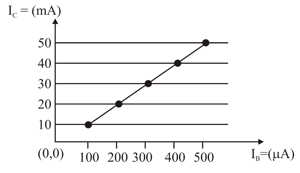
In an n-p-n common emitter (CE) transistor the collector current changes from to for the change in base current from and , respectively. The current gain of transistor is _____.
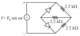
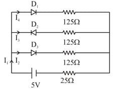
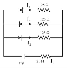
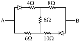
If each diode has a forward bias resistance of in the below circuit,
Which of the following options is correct?
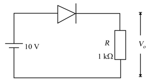
In the given circuit, the current through the battery will be
Given below are two statements: one is labelled as Assertion A and the other is labelled as Reason R
Assertion A: Diffusion current in a junction is greater than the drift current in magnitude if the junction is forward biased.
Reason R: Diffusion current in a junction is form the -side to the -side if the junction is forward biased.
In the light of the above statements, choose the most appropriate answer from the options given below.
The diagram shows the formation process of a p-n junction diode Identify the arrow representing
(i) Electron Diffusion
(ii) Electron Drift
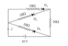
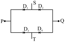
Following circuit contains diodes with forward bias having resistance and reverse bias having infinite resistance. The ratio of is equal to
In the given figure, a p-n Junction is

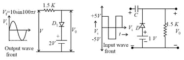
Alternating voltage is given across and , and output is taken across and Choose the correct option for output voltage.
In the given circuit, the equivalent resistance (in ) betweenand is (if has positive
potential and has negative potential) (Diodes are assumed to be ideal)
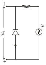
For the circuit shown in the figure, the output is
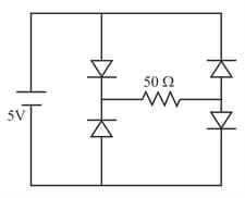
ideal diodes are connected as shown in the circuit, the current through is
Identify the incorrect statement with respect to depletion layer.
The increase in the width of the depletion region in a - junction diode is due to:
In the given circuit, the approximate value of voltage drop across is
Explain the operation of the following circuit with neat sketch of the input output waveforms. Consider all the diodes are ideal.

Determine output waveform, for the following networks considering all the diodes are ideal.
Explain the operation of the following circuit with neat sketch of the input output waveforms. Consider all the diodes are ideal.
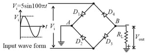
Sketch the voltage across the central resistor as a function of time. Take current in left direction as positive.